Tutorial IC Design
Table of Contents
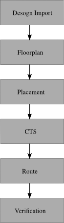
1 Place & Route design flow
1.1 Goals
The goal of this tutorial is to explain the physical design in more detail. In this tutorial, the physical design is developed for a small single-core RISC-V SoC; it is called PULPino.
You are going to exersice the following steps:
- Floorplanning
- Placement
- Clock Tree Synthesis
- Routing
- Verification
The general view of the flow is shown in the following picture:
1.2 Orginize your data and setup the tool
Before you start, it is a good idea to orginize your data by creating set of directories
where you are going to put the data generated during the design flow. Go to the directory
of pulpino_soc and create the following directories:
cd pulpino_soc/do_pr
mkdir results
mkdir reports
mkdir cmd
mkdir log
mkdir tool
For the lab you are going to use the INNOVUS tools from Cadence.
Create a sourceme.sh file to do the setup and copy the following commands into your file.
export LM_LICENSE_FILE=28211@item0096
source /eda/cadence/2017-18/scripts/INNOVUS_17.11.000_RHELx86.sh
Now you can source that file.
source sourceme.sh
And then, you can start the tool
innovus -log log/
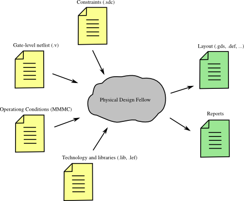
2 Design import
To move from logical to physical design you need to:
- Define the design (.v)
- Define design constraints (.sdc)
- Define operating conditions (MMMC)
- Define technology and libraries (.lef , .lib)
In order to provide the tool with the inputs, in the menu execute File → Import Design
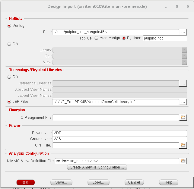
You have to select the gate-level verilog file of your design to read and then, specify the name of the top cell.
In additin, you have to set the LEF files with the information about the standard cells, and the power nets of your design,
i.e. VDD and VSS. In Analysis Configuration part, you need to set the timing libraries and constraints
by either importing a MMMC view definition file or clicking on Create Analysis Configuration ...
Click on Create Analysis Configuration ... :
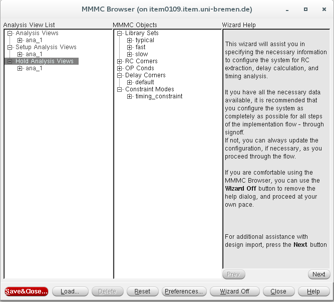
After setting the timing libraries and constraint file (.sdf), click on Save&Close
to save all settings in a .view file.
Alternatively you can execute the following tcl commands:
set init_lef_file {../../../0_FreePDK45/NangateOpenCellLibrary.lef ../../../0_FreePDK45/NangateOpenCellLibrary.tech.lef ../../../0_FreePDK45/NangateOpenCellLibrary.macro.lef}
set init_gnd_net VSS
set init_pwr_net VDD

set init_verilog ../gate/pulpino_top_nangate45.v
set init_top_cell pulpino_top

set init_mmmc_file pulpino_top.view

init_design
The .view file can be automatically generated as follows:
# Version:1.0 MMMC View Definition File
# Do Not Remove Above Line
create_library_set -name typical -timing {../../../0_FreePDK45/CCS/NangateOpenCellLibrary_typical_ccs.lib}
create_library_set -name fast -timing {../../../0_FreePDK45/CCS/NangateOpenCellLibrary_fast_ccs.lib}
create_library_set -name slow -timing {../../../0_FreePDK45/CCS/NangateOpenCellLibrary_slow_ccs.lib}
create_constraint_mode -name timing_constraint -sdc_files {../gate/pulpino_top.sdc}
create_delay_corner -name default -library_set {typical}
create_analysis_view -name ana_1 -constraint_mode {timing_constraint} -delay_corner {default}
set_analysis_view -setup {ana_1} -hold {ana_1}
3 Floorplan
3.1 Specify the floorplan
In this step, you should define the floorplan size, aspect ratio, target utilization of your unit.
In the menu select Floorplan → Specify floorplan.
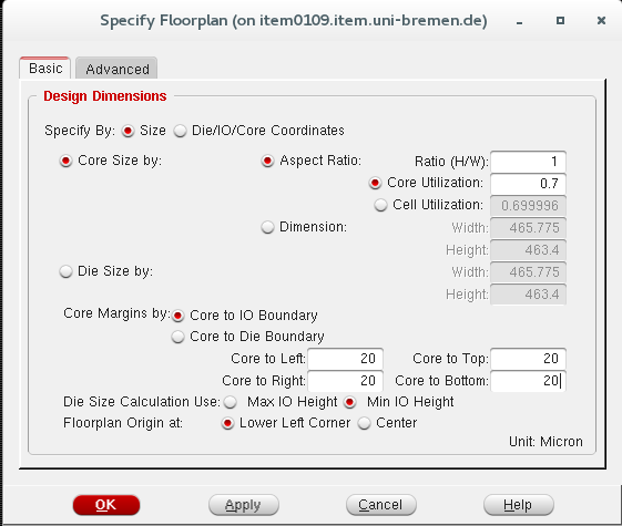
For example, you can select that the design should have an aspect ration of 1, a core utilization of 70% and a core to io boundary distance of 20 μ m in all the directions. Aspect Ratio defines the chip's core dimensions as the ratio of the height divided by the width. Core Utilization determines the core and module sizes by total standard cells and macros density.
Alternatively you can execute in the tcl terminal:
floorPlan -r 1 0.7 20.0 20.0 20.0 20.0
3.2 Hard macro placement
You can place the macros using the Move/resize/reshape (alternatively you can use: Shift + R) from the menu. Select the macros using your mouse and place them freely in your floorplan. When placing large macros, you must consider impacts on routing, timing, power, and particularly the position of the pins when placing large macros. Usually push them to the sides of the floorplan.
After roughly placing the macros, it should be legalized choosing Floorplan → snap Floorplan.
3.3 Power rings
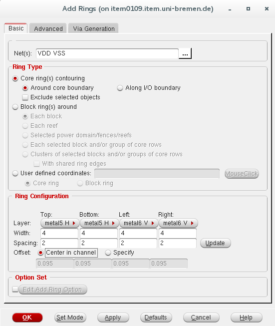
Often rings for VDD, GND are placed around the chip periphery, as well as around each individual hard IP.
In the next step, we add the powerrings around the core boundary. In the menu select Power → Power Planning → Add Ring.
Alternatively you can execute in the tcl terminal:
addRing -nets {VDD VSS} -follow core -stacked_via_top_layer metal10 -stacked_via_bottom_layer metal1 -layer {bottom metal1 top metal1 right metal2 left metal2} -width 3 -spacing 1
3.4 Pin assignment
Location of pins can be set with Edit → Pin editor. You can choose the pins and the side of
the floorplan in which pins should be located.
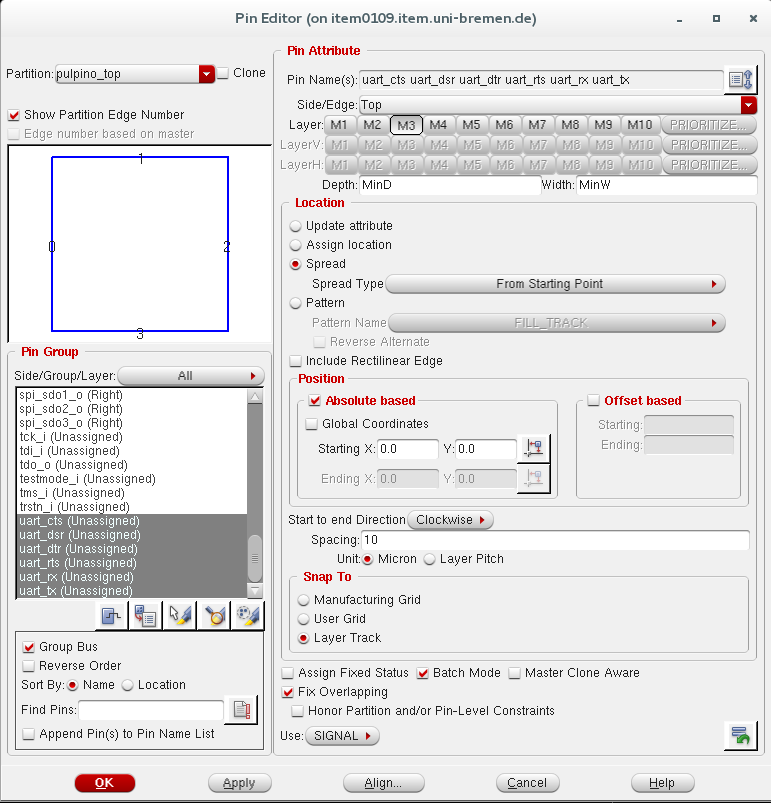
For example, you can select the uart pins and place them on Top side of the floorplan on metal 3. A 10 μ spacing
is considered between pins.
Alternatively you can execute in the tcl terminal:
editPin -fixOverlap 1 -unit MICRON -spreadDirection clockwise -side Right -layer 3 -spreadType start -spacing 10 -start 0.0 0.0 -pin {uart_cts uart_dsr uart_dtr uart_rts uart_rx uart_tx}
4 Placement
4.1 Standard cell placement
Now we can place the cells. In the menu slect Place → Place standard cells.
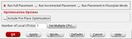
Deselect the Include Pre-Place Optimization and click in Mode... to select additional options.
In the new window you should select Place IO Pins.
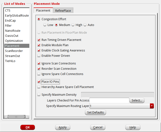
The equvallent tcl command is as follows:
setPlaceMode -placeIOPins 1
placeDesign -noPrePlaceOpt
4.2 Spare cell placement
Sometimes not everything works properly after tape-out. Spare cells are basically elements embedded in the design
which are not driving anything. The idea is that maybe they will enable an easy fix without
the need of a full redesign. In order to add some spare cells choose place → Place Spare Cell ....
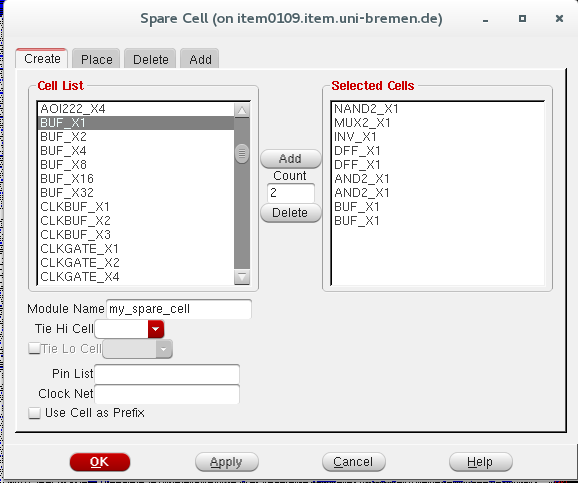
You can select some cells from the cell list and name the module.
Alternatively you can execute in the tcl terminal:
createSpareModule -moduleName my_spare -cell {AOI222_X4 1 BUF_X1 2 DFF_X1 5}
4.3 Filler cell placement
You should insert filler cells to fill the holes in the rows. However, it should usually done after routing and clocl tree synthesis in order to prevent congestion problem.
In the menu select Place → Physical cells → Filler cells.
Click in Select and select all the filler cells, then click ok.
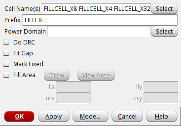
Alternatively, you can execute the following tcl command.
addFiller -cell FILLCELL_X8 FILLCELL_X4 FILLCELL_X2 FILLCELL_X1 -prefix FILLER
At this point, you can generates a timing report that provides information about the various paths in the design.
The report_timing command without the -unconstrained option reports only constrained
paths. If no constrained path is found, there may be unconstrained paths or the path may not exist.
Now, we report the timing of the design for unconstrained paths by defining the a delay limit and save the results in a file:
report_timing -unconstrained -delay_limit 20 > reports/timing_report_postPlace.rpt
5 Clock tree synthesis
So far we have designed a floorplan for physical implementation and provided a location for each and every gate. Until now, we have assumed an ideal clock. In this step, we have to provide all sequential elements with a real clock signal.
Clock net has a big impact on timing, power, area and etc. Therefore, we do not route clock net to all sequential elements just like any other net.
Clock Tree Synthesis (CTS) can automatically generate a clock tree specification from multi-mode timing constraints and then synthesize and balance clock trees to that specification. CCOpt (Concurrent clock optimization) tool extends CTS by adding cocurrent clock optimization, which simultaneously optimizes clock and datapath to achieve better performance, area, and power.
In order to do CCOpt, we use tcl command to set CCOpt as the clock synthesis engine.
Moreover, using the setDesignMode command you can specify a process technology value.
Setting the process technology leads to a more accurate RC extraction.
setCTSMode -engine ccopt
setDesignMode -process 45
Then, we set a target maximum transition time and a target skew:
set_ccopt_property target_max_trans 0.08
set_ccopt_property target_skew 0.5
Now, we can create the clock tree by defining a name for the clock tree and specifying the main clock pin. Finally, we run the concurrent clock tree optimization as follows:
create_ccopt_clock_tree -name MY_CLK -source clk
ccopt_design
Reports on clock trees and skew groups can be obtained using these CCOpt reporting commands:
report_ccopt_clock_trees –file reports/clock_trees.rpt
report_ccopt_skew_groups –file reports/skew_groups.rpt
After the clock tree optimization, again we report the timing of the design:
report_timing -unconstrained -delay_limit 20 > reports/timing_report_postCCopt.rpt
compare two timing reports.
6 Route the design
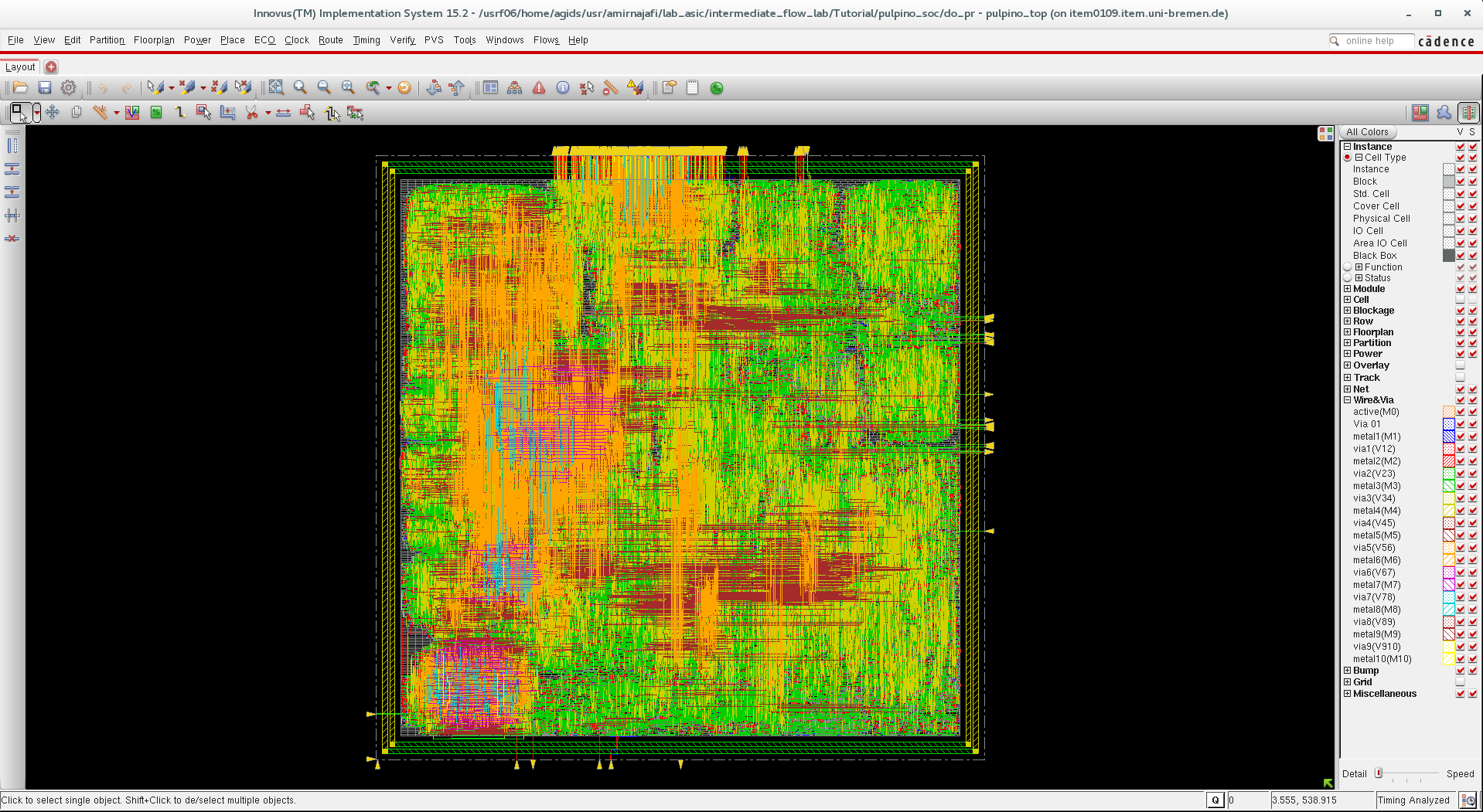
After the placement and clock tree synthesis, we can route the nets. In the menu select Route → Nano route → Route.
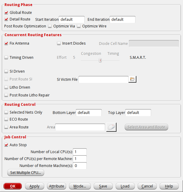
Alternatively, you can execute the following tcl command.
routeDesign -globalDetail
7 Verify and write result
You can check that your design does not have errors. In the tcl terminal type:
verify_drc   -report reports/pulpino_soc.drc
verify_connectivity -report reports/pulpino_soc.connect
You can as well choose verify → verify DRC ... from the menu.
Now you can export your design into a gds file. File → Save → GDS/Oasis.
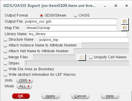
Alternatively, you can execute the following tcl command.
streamOut results/pulpino_soc.gds -mapFile streamOut.map -libName my_library -units 2000 -mode ALL